Aachen, August 21, 2019 - Electronic applications are an essential part of our everyday life and have led to the increasing digitalization of life and work processes in recent decades. Modern smartphones or tablet computers have the computing power that 50 years ago required computer centers in the size of entire buildings. Technical developments have led to increasing miniaturization and even to today's "lab on a chip".
With the "Printed Electronics" consortium project, KEX Knowledge Exchange AG offers interested companies the opportunity to gain insights into current and future developments in printed electronics, to determine the potential and opportunities for their own companies and to actively shape the next disruptive step in development themselves.
New fields of applications in the consumer and industrial sectors
Thanks to Printed Electronics, there is now a wide range of new product classes and applications such as flexible screens, smart labels, and packaging. Innovative electronic components - such as metallic temperature and level sensors, strain gauges or gas sensors - can be manufactured using the printed electronics process. Here, metal oxide semiconductor materials are printed, which are then used in further processing. Due to increasingly fine-grained substrates, printed components can be produced thinner, lighter, and more flexible. In addition to the steadily increasing demand for wearables and thinner and lighter electronics, printed electronics are also increasingly being used in the manufacture of flexible keyboards, antennas, and electronic skin patches.
Printed electronics also play an important role in the smart design of everyday objects: from sensors, resistors, and capacitors to entire displays and printed batteries, printed electronics are integrated into paper, plastic film, fabric, metals, and 3D print objects. That opens up a wide range of possibilities for electronic device applications, enriching many industries such as healthcare, aerospace, and transportation.
In addition to the technical advantages, aspects such as reduced costs, roll-to-roll production, and integration of individual components into assemblies by Printed Electronics ensure that the manufacturing process continues to gain in popularity and applications.
Modern production technology for complex electronics
The technical principle used in the production of printed electronics, which is already basically applied to "classically" manufactured circuit boards, is comparatively simple: conductive ink is applied to non-conductive substrates in a process similar to that of a classic printer, thus ensuring conductive paths. Whereas the printed circuit boards previously had to be post-processed using chemical and mechanical processes and fitted with additional functional components, in future printed electronics will make it possible to produce complete systems ready for installation.
Become part of our success story
In order to actively participate in the development of Printed Electronics, KEX Knowledge Exchange AG, is offering the second consortium project on printed electronics under the title "Printed Electronics" together with its research partners.
Renowned research institutions such as the Fraunhofer Institute for Manufacturing Engineering and Applied Materials Research IFAM, the Fraunhofer Institute for Production Technology IPT, the Fraunhofer Institute for Laser Technology ILT and the ACAM Aachen Center for Additive Manufacturing are looking forward not only to research current and future trends and technologies theoretically, such as low-cost electrification and smartification of products, together with interested industrial partners, but also to actively promote their practical implementation. As consortium partners, companies can actively shape the focus of the project and thus select and further develop the most relevant applications for their benefit.
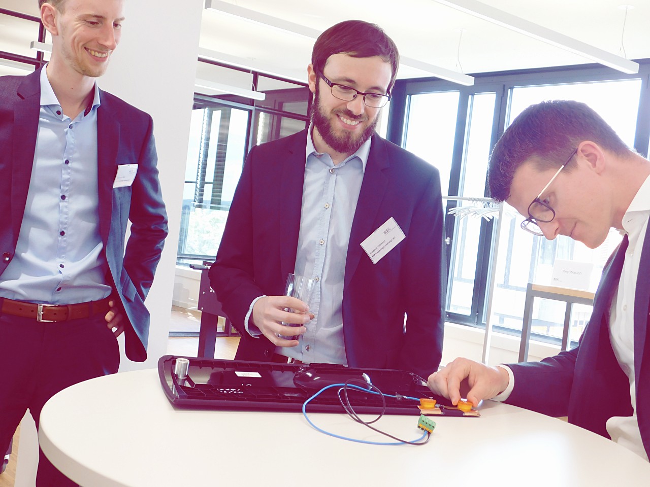
In the previous consortium project on "Printed Electronics", more than 40 possible technologies (e.g., roll-to-roll processes or additive manufacturing processes) and more than 300 applications (lighting, smart packaging, sensors, etc.) from various industries were identified. In addition, 2D applications (e.g. OLED lighting and HMI) and equally potential 3D solutions (e.g. space-saving, compact printed circuit boards or 3D printing of sensors on components) were successfully analyzed in detailed technology studies. At the same time, an initial prototype for an alternative e-heating concept was both developed and tested in cooperation with the consortium partners.
The Printed Electronics consortium project started today, August 21, 2019, as part of a kick-off. Interested companies still have time until 25.09.2019 to secure a place in the consortium.